Since digital data is usually stored in the form bits, digital memory devices such as the computer random access memory (RAM) requires a way for storing and switching between the two binary states. A flip-flop is a sequential logic device that can perform this operation. The flip-flop is called a bistable device, because it has two possible stable output states: 1 (high) and 0 (low). It has the capability to remain in a particular output state (storing a bit) until input signals cause it to change it. This forms the basis of all semiconductor information storage and processing in digital computers. In reality, flip-flops perform most of the basic functions critical to the operation of all digital devices.
RS Flip-Flop
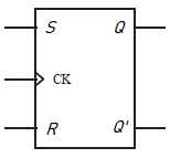
A schematic diagram of basic flip-flop, an RS flip-flop is shown in the figure below.

S is the set input, R is the reset input, and Q and Q’ are the complementary outputs. Most flip-flops include both outputs, where one output is the inverse (NOT) of the other. The RS flip-flop operates based on the following rules:
- As long as the inputs S and R, are both 0, the outputs of the flip-flop remain unchanged.
- When S is 1 and R is 0, the flip-flop is set to Q = 1 and Q’ = 0.
- When S is 0 and R is 1, the flip-flop is reset to Q = 0 and Q’ = 1
- It is not allowed (NA) to place a 1 on S and R simultaneously since the output will be unpredictable.
The truth table can be used to describe the functionality of a flip-flop. Let’s consider the truth table below:
Table 1.0 Truth table for the RS flip-flop
| Inputs | Outputs | ||
| S | R | Q | Q’ |
| 0 | 0 | Q0 | Q’0 |
| 1 | 0 | 1 | 0 |
| 0 | 1 | 0 | 1 |
| 1 | 1 | NA | |
The truth table above for a basic RS flip-flop is shown above. The first row shows the memory state where the flip-flop retains the last value set or reset. Q0 is the value of the output Q before the indicated input conditions were determined; 1 is the logic high and 0 is the logic low. The NA in the last row indicates that the input condition for that row is not allowed. Since we are barred from applying the S = 1, R = 1 input condition, the RS flip-flop is rarely used in actual digital logic designs. Other more flexible flip-flops that avoid the NA limitation are preferred like JK flip-flip.
The Internal Design of RS Flip-Flop
The internal design of an RS-flip consists of combinational logic gates with internal feedback from the outputs to the inputs of the NAND gates.

The figure below illustrates the timing of the various signals that are affected by very short propagation delays through the NAND gates.

Immediately after signal R transitions from 0 to 1, the inputs to the lower NAND gate are 0 and Q, which is still 1. This changes Q’ to 1 after a slight propagation delay Δt1. Feedback of the Q’ to the top NAND gate drives Q to 0 after a slight delay At2. Now the flip-flop is reset, and remains in this state even after R returns 0. The set operation functions in the same way. The propagation delays Δt1 and Δt2 are typically in the nanosecond range. All sequential logic devices depend on the feedback and propagation delays for their operation.
The Triggering of Flip-Flops
Flip-flops are normally clocked, i.e. a signal that is designated “clock” coordinates or synchronizes the changes of the output states of the device. This allows the design of complex circuits like a microprocessor where all the system changes are triggered by a common clock signal. This is called synchronous operation as changes in state are coordinated by the clock pulses. The outputs of different types of clocked flip-flops can change on either a positive edge or a negative edge of a clock pulse. These flip-flops are referred to as edge-triggered flip-flops. Positive edge triggering is specified schematically by a small angle bracket on the clock input to the flip-flop. Negative edge triggering is specified schematically by a small circle and angle bracket on the clock input. Check the figures below:
Take note of the small circle and angle bracket for the negative edge triggered RS flip-flop below to distinguish from the positive-edge triggered RS flip-flop above.
")
The truth table for a positive edge-triggered RS flip-flop is given in the Table 1.1 below. The up arrow ↑ in the clock (CK) column represents the positive edge transition from 0 to 1. The NA in the second to last row specifies that the input condition for that row is not allowed. As long as there is no positive edge transition, the values of S and R have no effect on the output as indicated by the X symbols in the last row of the table.
Table 1.1 Positive-edge-triggered RS flip-flop Truth Table
| S | R | CK | Q | Q’ |
| 0 | 0 | ↑ | Q0 | Q’0 |
| 1 | 0 | ↑ | 1 | 0 |
| 0 | 1 | ↑ | 0 | 1 |
| 1 | 1 | ↑ | NA | |
| X | X | 0,1,↓ | Q0 | Q’0 |
A typical example of timing diagram is illustrated below. The output is reset (Q=0) at the first positive edge of the clock signal, where R = 1 and S = 0, and the output is set (Q = 1) at the second positive edge, where S = 1 and R = 0.

The operation of the edge-triggered RS flip-flop is defined by the following rules:
- If S and R are both 0 when the clock edge is encountered, the output state remains unchanged.
- If S is 1 and R is 0 when the clock edge is encountered, the flip-flop output is set to 1. If the output is at 1 already, there is no change.
- If S is 0 and R is 1 when the clock edge is encountered, the flip-flop is reset to 0. If the output is at 0 already, there is no change.
- S and R should never both be 1 when the clock edge is encountered.
Latch
A latch (e.g. D latch) is an example of special devices that are not edge triggered as described above. The schematic symbol of a latch is shown below:
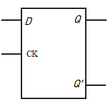
In the operation of a latch, the output Q tracks the input D as long as clock (CK) is high. When a negative edge occurs, that is when CK goes low), the flip-flop will store (latch) the value that D had at the negative edge, and that value will be retained at the output. Since the output follows the input when the clock is high, that latch is said to be transparent during this time. The latch can also be called a positive-level-triggered device. The truth table for a latch is given below:
Table 1.2 Latch Truth Table
| D | CK | Q | Q’ |
| 0 | 1 | 0 | 1 |
| 1 | 1 | 1 | 0 |
| X | 0 | Q0 | Q’0 |
The timing diagram is shown below:

D Flip-Flop
The D flip-flop is also referred to as a data flip-flop, and has a single input D whose value is stored and presented at the output Q at the edge of a clock pulse. A positive edge-triggered D flip-flop is demonstrated in the Figure 1.8 below.

Unlike a latch, a D flip-flop does not exhibit transparency. The output changes only when triggered by the appropriate clock edge (in this case, a positive edge).
Table 1.3 Positive-edge-triggered D Flip-flop Truth Table
| D | CK | Q | Q’ |
| 0 | ↑ | 0 | 1 |
| 1 | ↑ | 1 | 0 |
| X | 0 | Q0 | Q’0 |
| X | 1 | Q0 | Q’0 |
JK Flip-Flop
The JK flip-flop is similar to the RS flip-flop where the J is analogous to the S (set) input and the K is analogous to the R (reset) input. The key difference is that the J and K inputs may both be high at the same time. This state causes the output to toggle, which means the output changes value, that is, 1 would become 0 and a 0 would become 1. The schematic symbol of JK flip-flop is shown below:

The truth table for a negative-edge-triggered JK flip-flop is given below:
Table 1.4 Negative-edge-triggered JK flip-flop Truth Table
| Operation Mode | CK | J | K | Q | Q’ |
| NO CHANGE | ↓ | 0 | 0 | Q0 | Q’0 |
| SET | ↓ | 1 | 0 | 1 | 0 |
| RESET | ↓ | 0 | 1 | 0 | 1 |
| TOGGLE | ↓ | 1 | 1 | Q’0 | Q0 |
| NO NEGATIVE-EDGE | 0,1 | X | X | Q0 | Q’0 |
The symbol ↓ represents the negative edge of the clock signal, which causes the change in the output. The last low describe memory feature of the flip-flop in the absence of a negative edge.
Asynchronous Inputs
Flip-flops may have preset and clear functions that instantaneously override any other inputs. They are referred to as asynchronous inputs, since their effect may be asserted at any time. They are not triggered by a clock signal. The preset input is used to set or initialize the output Q of the flip-flop to high (1). The clear input is used to clear or reset the output (Q) of the flip-flop to low (0). The small inversion symbols indicated at the asynchronous inputs means that the function is asserted when the asynchronous input signal is low. Such an input is termed to as an active low input. Both preset and clear should not be asserted at the same time. Either of these inputs can be used to define the state of a flip-flop after power-up; else at power-up the output of a flip-flop is uncertain.

Related articles:
- What is a Microprocessor Clock?
- CPU Registers
- Multiplexers and Demultiplexers in Digital Circuits
- Basic Features of a Microprocessor-Based System
- What is a Microprocessor?
Related resource: Encyclopedia of Electronic Components for Your Project
Leave a Reply
You must be logged in to post a comment.